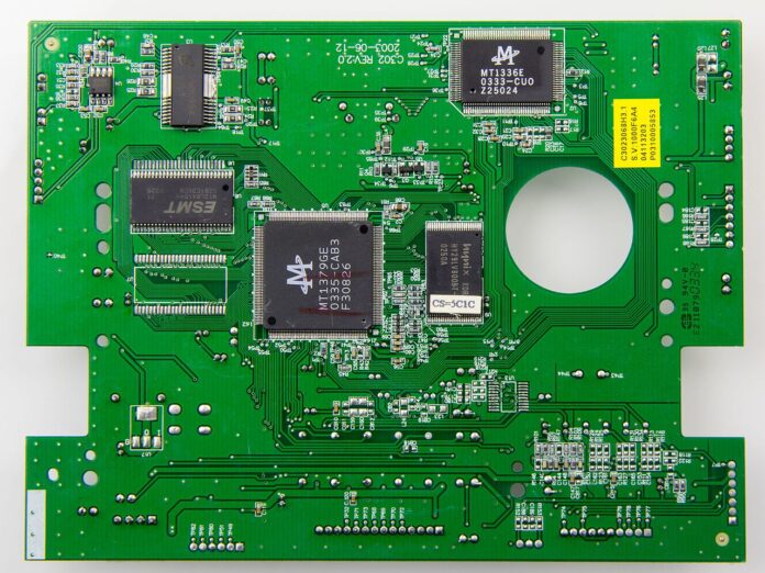
PCB – Printed Circuit Board is a device that everyone has seen but is totally unaware of.
We often call it as a circuit board, and people recognize it by the green colour it has with
yellow strips on it. You must have seen such a circuit board in your electronic devices like TV sets, Computers, Gaming consoles, remote control sets, etc., and at least once in our lifetime, we have taken it out either for repairing purposes or for checking some loose
connections or soldering problems.
But apart from that, we do not have any knowledge about it, so in this article, we will
have some information on high density PCBs. But before that, first, let us understand what PCB is.
What is PCB?
PCB or Printed Circuit Board is a laminated structure of conductive and insulating
layers that are sandwiched together on the board. The PCB is considered to be the
foundational block for several electronic devices, including conventional as well as
modern electronics.
These circuit boards have two complementary functions; the first one is to affix the
electronic components in the respective locations on the board’s outer surface by
soldering. The second function is to provide reliable electrical connections and open
circuits between the component’s terminals in a controlled manner.
Each of these conductive layers is designed with a pattern of conductors that caters to
the electrical connections on the said conductive layers. Another factor that proves the
credibility of these circuit boards or PCBs is the fact that it provides mechanical support
to the electronic components using the conductive pads that are designed in order to
accept the component’s terminals and connect them electrically using the traces, planes
and other copper layers that are laminated onto the circuit board.
High Density Interconnect PCB –
The high density interconnects PCB, shortly called HDI PCBs, are basically an upgraded
version of PCB. These High density interconnect PCBs have a higher circuitry density
per unit compared to conventional PCBs.
Such High density interconnects PCBs use a combination of buried and blind vias and
micro vias that are 0.006″ or less in diameter. Along with this, the high density
- interconnect PCBs are the advanced version of the conventional PCBs that has the
- following connection features –
- Through vias and buried viasThrough vias from surface to surface
- Minimum two layers with vias
- Coreless construction with layer pairs
- Passive substrate constructions with no electrical connections
- Alternative constructions with layer pairs
- The said high density interconnect technology in the conventional PCB is proving to be a
- critical driver in developing many high-end electronic devices that are small in size and
- weight.
- Now, after all this information, let us know some of the key benefits of using the high
- density interconnect technology in printed circuit boards or PCBs.
Key Benefits of High Density Interconnect PCBs –
Reduced size and weight –
HDI boards allow you to mount components on both sides of the bare PCB, reducing the
size and weight of your equipment while increasing its functionality. You can improve
your product’s functionality using HDI technology even as you shrink its physical
footprint.
Improved Performance –
When the distance between components is reduced, and the number of transistors is
increased, the electrical performance of the device can be enhanced. Together, these
signal integrity and efficiency enhancements result in significantly reduced power
consumption. We can expect faster signal transmissions and larger reductions in overall
signal losses and crossing delays as sizes are reduced.
Cost Effectiveness –
With lower material costs due to their smaller size and fewer required layers, HDI
boards can be manufactured at a lower cost than alternatives if care is taken during the
design and production phases. A single HDI board may be sufficient for a product that
previously needed multiple conventional PCBs. Reduced space and quantity of material
are required to accomplish the same or greater level of performance and benefit.
Expediting the Manufacturing Process –
Design efficiencies associated with HDI technology can lead to faster production times
and a shorter timeframe needed to get your product to market, while the ability to use
fewer materials can lead to faster production times and a shorter timeframe. HDI
printed circuit boards have a high electrical performance that makes it easy to place
components and shortens the testing and troubleshooting phases.
Reliability –
The improved reliability of your board and final product can be attributed to the smaller
aspect ratios and higher quality construction of micro vias. HDI PCB’s increased
efficiency and dependability will help businesses save money while giving their
customers a better experience.
So, as we have discussed PCBs and HDI PCBs along with the benefits associated with
them, we can conclude that the HDI PCBs are the need of the time that assists the ever-
growing technology by producing some really advanced electronic devices.
Also Read About
Electrical Upgrades You Will Want for Your Home Remodel
How Can Electronic Signature Technology Benefit Your Business?
How to Recover Deleted Videos from the Pen Drive
10 Best ACs to Get low power Consumption within India (from 2022): Review and the full guide
Invest in Green Hydrogen Economy Watch Hydrogen Stocks


